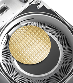
Conductor etch helps shape the electrically "active" materials used in the parts of a semiconductor device. Even a slight variation in these miniature structures can create an electrical defect that impacts device performance. In fact, these structures are so tiny that etch processes are pushing the boundaries of the basic laws of physics and chemistry.
Lam's Kiyo product family delivers the high-performance capabilities needed to precisely and consistently form these conductive features with high productivity.
